Synthesis, Processing, Properties and Application of 2D Materials
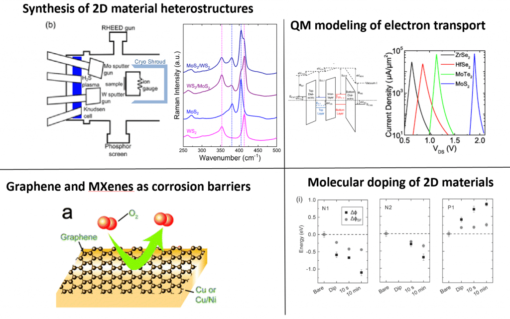
Two-dimensional materials such as graphene, transition metal dichalcogenides (e.g. MoS2) and transition metal carbides (e.g. Mo2C) have attracted significant interest in recent years due to their unique electronic, optical and chemical properties. There is a wide compositional space leading to wide ranging properties (metals, semiconductors, insulators), they have potential for monolayer thickness control leading to ideal quantum wells and ultrathin diffusion/permeation barriers, they ideally lack surface dangling bonds meaning heterostructures can be more easily formed, and they are flexible and can potentially be synthesized or transferred onto arbitrary substrates. While synthesis methods have been developed for 2D materials, many of these techniques require synthesis temperatures of 800 °C or higher. As a result of the thermal budget, direct synthesis requiring high temperatures is incompatible with many of the underlying substrates. Prof. Vogel’s group has developed low-temperature, plasma assisted, cyclic synthesis methods for transition metal dichalcogenides such as MoS2 [2D Materials 5, 015005 (2017); Journal of Vacuum Science and Technology B 36, 031201 (2018)] and developed a fundamental understanding of the kinetics and thermodynamics associated with synthesizing high quality Mo2C [2D Materials7, 035022 (2020)]. Prof. Vogel’s group has also explored the impact of the structure and bonding of 2D materials on their properties and application. For example, few-layer p-type WSe2 with wafer-scale thickness uniformity was synthesized leading to high-quality and uniform electronic properties [Nanoscale 8, 2268-2276 (2016)]. Both experimental and theoretical (quantum mechanical simulations) work has shown that heterostructures of 2D materials can lead to interesting electronic properties not achievable with conventional three dimensional materials [Journal of Applied Physics 119, 024503276 (2016); ACS Applied Materials and Interfaces 8, 8702-8709 (2016); IEEE Transactions on Electron Devices 64, 2714-2720 (2017); ACS Applied Materials & Interfaces 10, 39860-39871 (2018); IEEE Transactions on Electron Devices 64, 2714-2720 (2017)].
Surface Interactions and Application of Electronic Biosensors
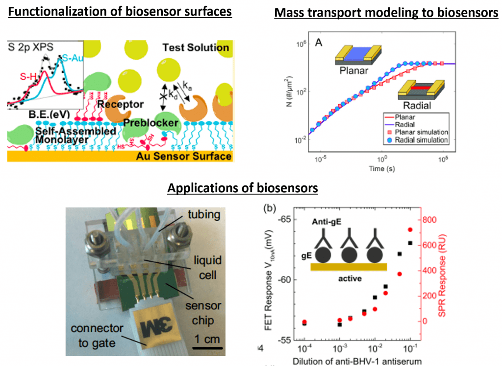
Currently, diagnosis for serological diseases such as Ebola, HIV, and Lyme disease relies on Enzyme-linked Immunosorbent Assays (ELISAs), which require centralized laboratories and several-day timescales to complete. However, emerging technologies such as potentiometric and electrochemical impedance biosensing can be developed into portable, label-free, point-of-care devices that require only hour timescales. Specifically, potentiometric sensing platforms can be miniaturized through cost-effective microfabrication, lend themselves to multiplexed and parallel sensing, and are easily integrated with other electronics. Despite the promise of these new technologies, device reliability inhibits commercialization and adoption. Prof. Vogel’s group pursues fundamental research related to the materials and interaction of the sensor surface with the biological solution as well as the use of these sensors in a variety of applications.
For example, mass transport to the sensor surface is a critical step in biosensing, often being the factor determining the limit of detection. Modeling transport of the analyte to a surface under convection and diffusion is a challenging task often requiring complex simulation. Prof. Vogel’s group developed a general model for mass transport to planar and nanowire biosensors under flow that is applicable over a wide range of variables [Journal of Applied Physics 125, 114502 (2019)]. Overall, the results provided a fundamental understanding and strategies for improving the detection limit of biosensors. As another example, although commonly used to functionalize the sensing surface, carboxyl-terminated thiol self-assembled monolayers (COOH-SAM) can have large defect densities, which in turn leads to large non-selective adsorption (NSA) of proteins to hydrophobic surfaces exposed by these defects. A procedure was developed where the surface of COOH-SAMs is treated before functionalization to improve the reliability and quality of receptor attachment to the sensor surface [Journal of Physical Chemistry C 123, 16778-16786 (2019)]. In this method, a pre-blocking protein orthogonal to the immunological system of interest is used to cover hydrophobic, non-selective sites on the sensor surface while still leaving carboxylic acid headgroups available for covalent functionalization. Haptoglobin detection via surface plasmon resonance with a pre-blocked aHp sensor was shown to perform similarly to conventional post-blocking, while demonstrating improved baseline stability and percentage of active receptors. Beyond this more fundamental research, the group has active projects associated with applying these sensors to a variety of use cases including development and validation of an on-farm, electronic disease diagnosis platform for cattle, sensor capsules for real-time measurement of cell properties in bioreactors, and next-generation sensors for stand-alone identification of biological weapons of mass destruction.

Metal Oxides for Bio-inspired Memory Applications
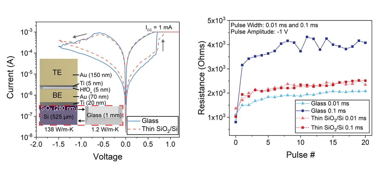
As part of an AFOSR MURI project funded in 2017 entitled, “Cross-disciplinary Electronic-ionic Research Enabling Biologically Realistic Autonomous Learning (CEREBRAL),” Prof. Vogel and his group have been collaborating with GT ECE, ME and SUNY Binghamton to fundamentally understand and develop a variety of adaptive oxides for use as analog memory in neuromorphic computing applications; computing in a way similar to the mammal brain. Prof. Vogel’s group has focused on filamentary adaptive oxide devices based on HfOx whose time-dependent resistance depends on the concentration of oxygen vacancies in the filament region. A local temperature rise from joule heating associated with an applied current plays a significant role in the movement of oxygen ions, making thermal management crucial to reliable performance. To date, the group has developed a fundamental understanding of how thermal transport impacts stoichiometry and resistance change in these materials [Journal of Materials Chemistry C 8, 5092-5101 (2020); Applied Physics Letters 116, 063504 (2020)].

Materials and Processes for Nano-modular Devices for Desktop Integrated Circuit Manufacturing
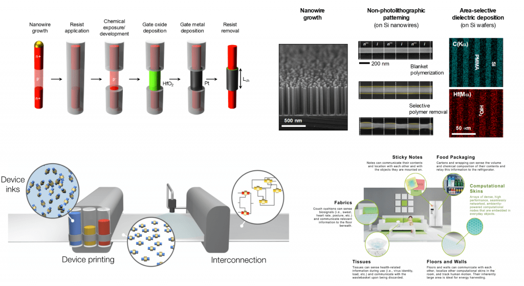
In 2015, Prof. Vogel started a new, highly interdisciplinary collaboration with a group of faculty including Prof. Michael Filler (ChBE), Prof. Gregory Abowd (CoC), and variety of other faculty at GT and elsewhere. The initial concept was that recent advances in materials science and manufacturing allow us to foresee a time when we really will be able to produce everyday materials with computational capabilities “woven” into them – an “Internet of Materials” (IoM). If we push on manufacturing processes so that generating a computing element (e.g., a transistor, memory bit) is as cheap as producing a molecule of aspirin, we can begin to imagine a world in which every physical object has some computational capability. The overarching challenge has been that state-of-the-art ‘fabs’ cost well over $10B and development costs are increasing at a rate of 50% per microprocessor generation. To overcome these limitations, Prof. Vogel and his collaborators have proposed and are developing a series of new chemical processes to modularize nanoelectronic devices and, in doing so, enable the printing of high-performance ICs in a distributed and on-demand fashion [ACS Nano 14, 282-288 (2019)]. The concept is much like that of 3D printing which has revolutionized manufacturing by lowering the barrier to entry in manufacturing of primarily mechanical parts. These ideas have been used for several proposal submissions including one that has been recently funded. In 2020, DARPA organized a workshop around the idea of desktop manufacturing of ICs, and Profs. Vogel and Filler have submitted a proposal to DARPA for a seedling project.
